[Learnings] FETs & Analog Electronics
0. Foreword
This note provides a glimpse into the modern morphology of analog electronics and RF semiconductor devices. Most textbooks typically begin with low-level prerequisites, such as Kirchhoff’s circuit laws, Thévenin equivalent circuits, and band theory in semiconductors. While it may be an appropriate way for most learners, those who major in physics or have some experience with solid-state materials don’t really need this level of guidance. In fact, this old-fashioned approach isn’t very efficient when you need a quick refresher on analog electronics circuit design.
In the following sections, we’ll dive straight into field-effect transistors (FETs) and then move on to some typical amplifier circuits. Bipolar junction transistors (BJTs) aren’t chosen as an entry point for this note, unlike most textbooks, which claim they’re quickly becoming obsolete. As of 2026, the market has largely been taken over by metal–oxide–semiconductor field-effect transistors (MOSFETs) for fast-switching and insulated-gate bipolar transistors (IGBTs) for high-power handling. However, this excuse doesn’t hold water in certain specific fields where BJTs remain widely used – often due to their robustness and low cost.
1. Field-effect Transistors
1.1 Some History
I don’t plan to overburden this note with too many documentaries and fairytales, but it’s worth mentioning the etymology of the word “transistor”, which may help us develop a clear understanding of the underlying physics.
It’s also interesting to collect some surprising trivia and fun facts below
- The concept of FETs was actually first patented in 1925, 17 years earlier than the first observation of transistor effect in the point-contact transistor in 1947.
- The first BJT was invented by W. Shockley in 1948.
- JFET is the first device to be successfully built by J. Nishizawa and Y. Watanabe in 1950, but in the mid-1950s BJTs were the main stream due to FETs’ fabrication difficulty.
- ~ To be updated :) ~
1.2 Basic Concepts
First, we introduce the typical structure of an N-type MOSFET
- MOS: Metal-oxide-semiconductor sandwich, oxide layer typical thickness (1~10 nm).
- Channel: Narrow path where the charge carriers can flow through, controllable by voltage.
- Source: The terminal where the charge carriers enter the channel.
- Drain: The terminal where the charge carriers leave the channel.
- Gate: The terminal where a voltage is applied to control the channel’s on/off.
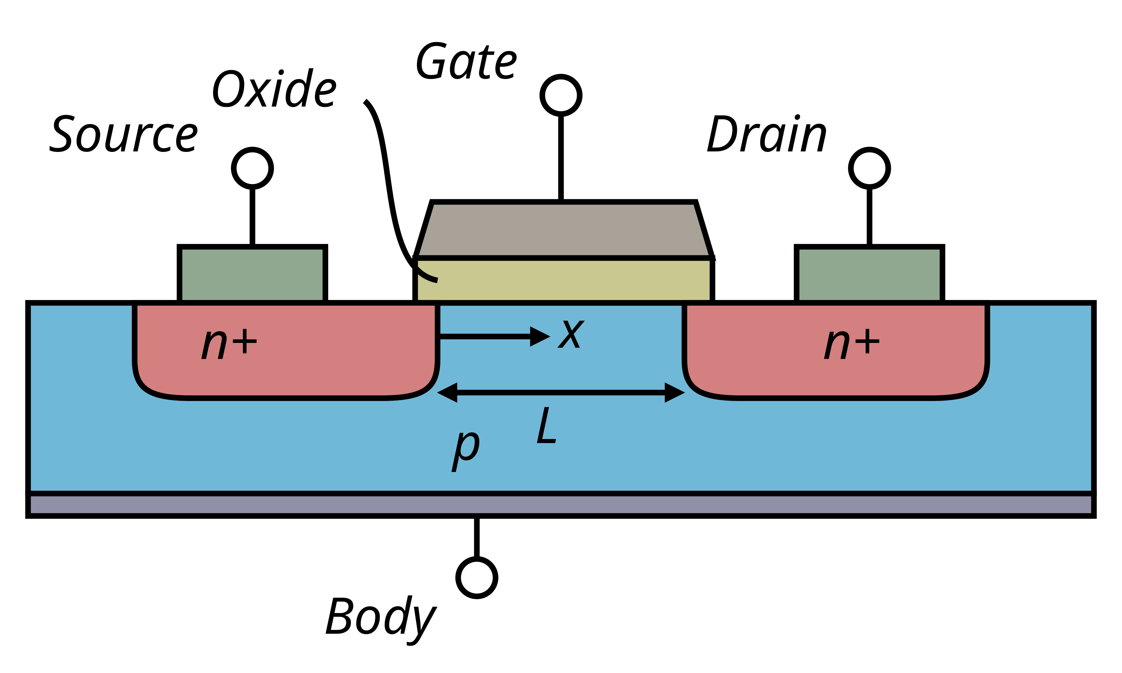
There are typically 3 terminals in a MOSFET, essentially 2 independent voltages. Usually we choose the source as our voltage reference. In other words, the 2 degrees of freedom (DoFs) are assigned to \(V_\text{DS}\) and \(V_\text{GS}\). The following situations arise when playing with these parameters
- \(V_\text{GS}=0,\, V_\text{DS}\neq 0\): At least one out of the two PN-junctions are reversely biased. The depletion layer of that junction becomes thicker and blocks the current.
- \(0<V_\text{GS}<V_\text{th},\, V_\text{DS}= 0\): Positive charges begin to accumulate on the gate, attracting more negative carriers in the P-type substrate, which depletes the area underneath. The channel becomes even more insulated at first. But when the depletion saturates, free electrons from the source and drain begin to creep into the channel. It forms a layer called inversion layer.
- \(V_\text{GS}=V_\text{th},\, V_\text{DS}=0\): The two separated inversion layers touch each other and form the channel. The voltage is referred to as the threshold voltage.
- \(V_\text{th}<V_\text{GS},\, 0\leq V_\text{DS}< V_\text{GS}-V_\text{th}\): The electron density in the channel is proportional to \(V_\text{GS}-V_\text{th}\). When the gate voltage increases, the channel becomes more conductive. Therefore, if applying drain-source voltage, current will begin to flow in the channel. But the channel width decreases from the source to the drain, since \(V_\text{GD}<V_\text{GS}\).
- \(V_\text{th}<V_\text{GS},\, V_\text{DS}=V_\text{GS}-V_\text{th}\): We find \(V_{GD} = 0\) and the channel width drops to 0 at the drain. The status is called pinch-off.
- \(V_\text{th}<V_\text{GS},\, V_\text{GS}-V_\text{th}<V_\text{DS}\): If we keep increasing the drain-source voltage, the current won’t drop although the channel has been pinched off. A tiny slit with strong electrical field will appear around the drain, where electrons in the channel will fleet towards the drain. In this region, the gate voltage \(V_\text{GS}\) has strong control on the channel current \(I_\text{D}\). Therefore, majority of the MOSFET-based amplifiers work in this region.